XTPL to deliver its Delta Printing System to ONTOS INC in the USA for semiconductor packaging developments
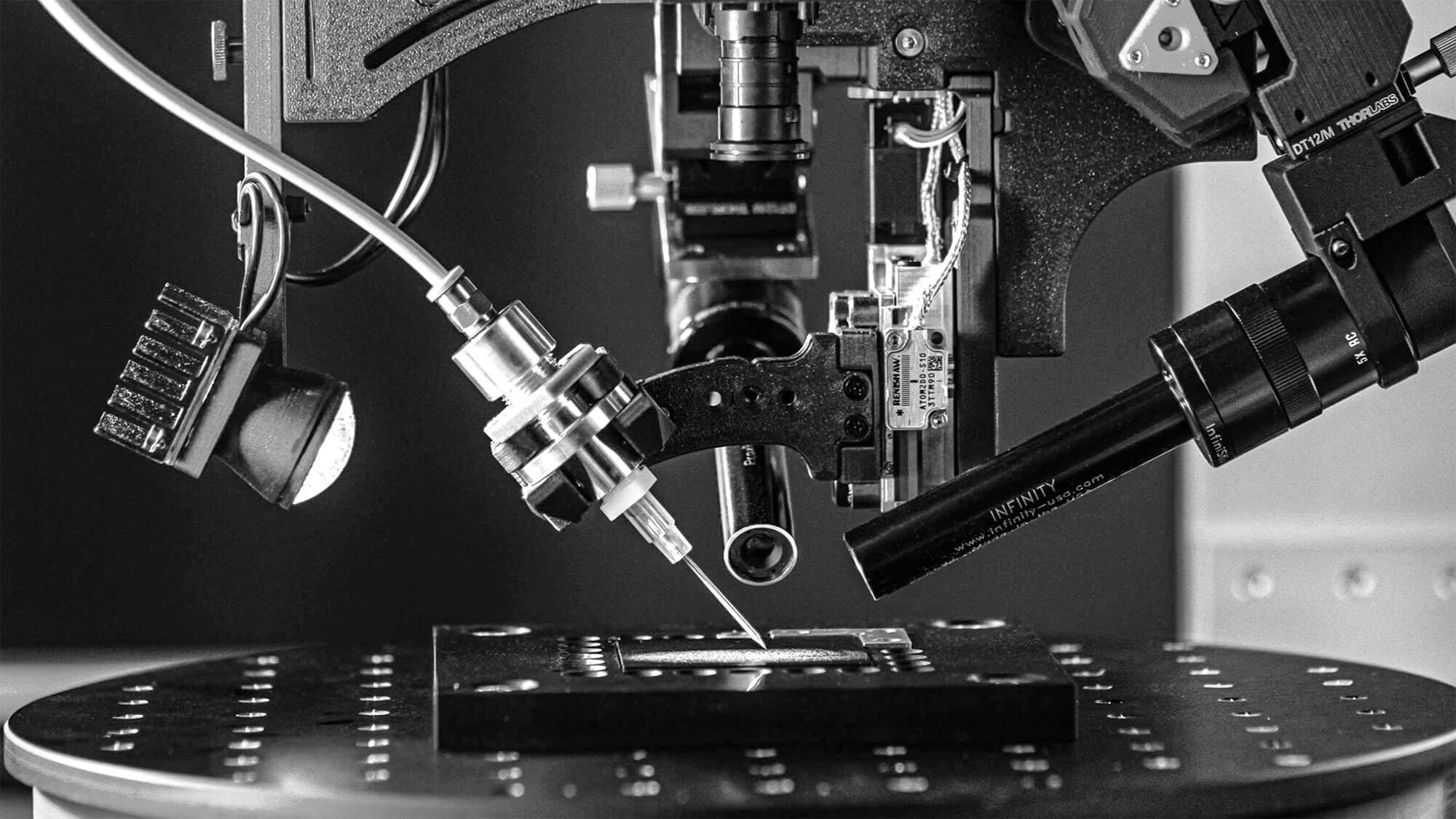
With another order for its Delta Printing System (DPS) prototyping device XTPL strengthens its collaboration with the US company ONTOS Equipment System Inc., which has been the distributor of XTPL’s technological solutions in North America since October this year. The DPS will be used in the R&D laboratory of ONTOS and its partners in the USA for advanced packaging of semiconductor chips, particularly in the hybrid bonding area. XTPL is to deliver and commission the DPS in the first half of 2024.
Based in Chester, New Hampshire, on the east coast of the United States, ONTOS Equipment System Inc. manufactures innovative equipment for surface preparation using atmospheric plasma at room temperature. ONTOS products are particularly used in prototyping and producing advanced integrated circuits. The company sells its products and services in more than 20 countries around the world. As XTPL’s official distributor in the North American market, ONTOS promotes the XTPL technology among its current customers as a solution that helps keep costs down and shortens the time of prototyping and small-scale production of advanced integrated circuits, as well as among its new customers as a complementary solution for making reliable electrical connections in semiconductors.
“Started in October 2023, the collaboration between ONTOS and XTPL is a major step towards innovation in the semiconductor industry. By combining the XTPL Ultra Precise Dispensing technology and the ONTOS Atmospheric Plasma technology, we will seek to leverage their potential in semiconductor packaging developments, particularly in the hybrid bonding area. This joint initiative is important especially now, when the semiconductor manufacturing independence both in the USA and in Europe is gaining more attention. Under the CHIPS and Science Act in the USA and the European Chips Act in Europe, advanced packaging challenges in the semiconductor industry are recognized among the top priorities” says Matthew Phillips, CEO of ONTOS Equipment Systems Inc.
The European Chips Act is an EU initiative designed to strengthen the European position in the semiconductor industry. Its main goal is to increase the EU’s global market share in chip production from 10% to 20% by 2030. A record EUR 43 billion is to be mobilized to enhance EU’s competitive position in this area. The CHIPS and Science Act in the USA was enacted in 2022 and its aim is to boost domestic manufacturing of semiconductors. It authorizes funding of USD 280 billion over 10 years to ensure that the United States regains its leadership position in the global semiconductor industry and increases the independence of its supply chains.
“Advanced packaging in the semiconductor field is one of our strategic verticals and markets for XTPL technology. So we are all the more honored and excited to collaborate with our partners at ONTOS, who have a long and rich experience in that industry. The delivery of our DPS to the ONTOS R&D lab in the USA will support the growth of the XTPL business in the American market and generally in the semiconductor industry. This will be another demonstration of XTPL technological capabilities in this key geography with a significant exposure to international customers and partners of ONTOS. This collaboration is in line with our strategy for the years 2023–2026, and I trust it will create new business growth opportunities for XTPL” comments Filip Granek, CEO of XTPL S.A.
XTLP started the commercialization of its Delta Printing System prototyping devices late in 2020/ early in 2021. By December 18, 2023, XTPL confirmed a total of 24 orders for DPSs, including 12 orders in 2023. The unit price of a DPS is approx. EUR 170–200 thousand.
XTPL’s strategy for 2023–2026 zooms in on two main areas of operations. The first area is developing business and sales in order to achieve commercial revenues of PLN 100 million by the end of 2026 and achieving the first implementations of the XTPL technology on an industrial scale. In addition, the Company’s plan is to expand its projects to include new industries – telecommunications and biosensors, continue to expand the international distributor network, and establish physical sales centers in technologically key destinations: the United States, Taiwan and South Korea. The second area is operational development and the development of the entire organization in order to significantly increase production capacity in all three business lines, as well as continuation of R&D on the existing portfolio and future products of the Company. This will be accompanied by the adaptation of the organization’s structure by streamlining internal processes with a view to building a strong brand with a tailored proposition and targeted markets. The Company also expects to strengthen and expand its competences by attracting new talent.
XTPL’s business model is based on three complementary business lines. These are printing modules for industrial implementation on the production lines of global manufacturers of electronics, the Delta Printing System (DPS) prototyping devices, and High Performance Materials (HPM, nanoinks). The Company has a total of nine projects aimed at industrial implementation of its technology, four of which are at an advanced stage of development. They cover three areas the Company considers strategic: semiconductors, displays and advanced PCBs. The potential average annual revenues from all nine industrial projects being developed at present totals an estimated PLN 400 million. The Company’s end customers are global entities responsible for the production of next generation electronics, including a leading semiconductor manufacturer from Taiwan, one of the world’s largest producers of FPDs (Flat Panel Displays) from South Korea and a top manufacturer of industrial machines from the United States, listed on the Nasdaq 100 index.