General Information
BUSINESS PROFILE
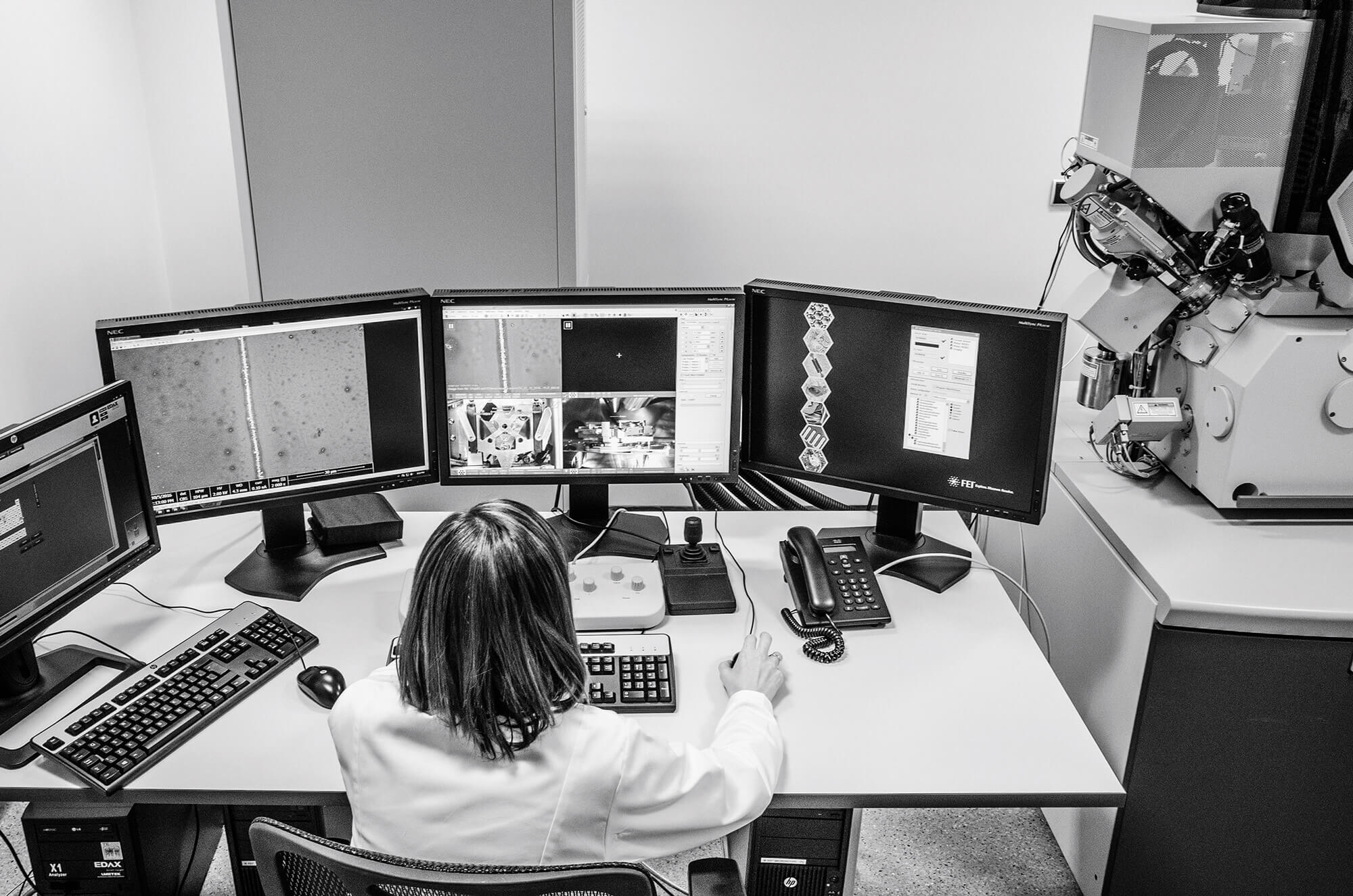
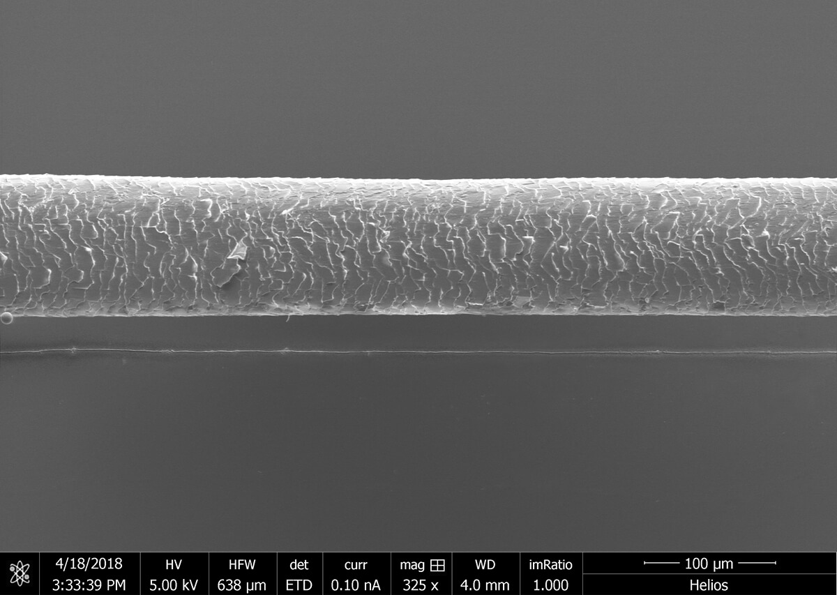
XTPL operates in the nanotechnology market segment. The company is developing and commercialising its globally innovative platform technology of ultra-precise printing of nanomaterials, protected by international patent applications. The XTPL method is a breakthrough. This is because of a unique combination of several features: it is an additive method, which ensures significant time and material savings and allows the advantages of print – such as scalability, cost effectiveness, simplicity and speed – to be used in the production of advanced devices thanks to unprecedented precision and without a need to use electric field. Due to its platform character, this solution will find application in the broadly understood printed electronics industry.
At present, the company is focusing on commercialization of its technology in chosen application fields. The first one is displays – here XTPL in the first step intends to offer the technology for repairing open defects of conductive structures, which are, among others, responsible for dead pixels occurring in high resolution matrices of displays already at the production stage. Next, the company plans to provide this industry with solutions that will help achieve a significant increase in the resolution of a new class of displays and the technology allowing for the production of displays on flexible substrates.
The second potential application field for XTPL is the smart glass market, i.e. glass that changes its transparency depending on external conditions.
For this sector XTPL intends to develop a solution that will significantly shorten the time of this conversion, which will highly improve the usability of such products, and may also usher the industry into new, not yet supported market segments.
The third area, developed since the first quarter of 2020, is the semiconductor industry. The company conducts R&D works in the field of creating ultra-precise conductive connections for semiconductor components present in lighting devices with one of the world leaders of this market. The lighting industry has been moving towards increasing the use of light-emitting semiconductor materials that convert electricity into light for many years. They are used in LED and OLED lighting. XTPL can have a significant role to play in this regard.
In the long perspective, the company intends to develop its solution for subsequent market segments. XTPL technology may be implemented in the above mentioned semiconductor industry also as a sought-after alternative for photolithography and, for example, facilitate the fabrication of innovative anti-counterfeiting solutions, advanced PCBs, functional and effective biosensors and high-performance photovoltaic panels. The technological revolution in which the company is to play a vital role is about enabling the production of complex and complicated electronic devices using cost effective and scalable printing methods.
BUSINESS MODEL
XTPL is a supplier of advanced technology of ultra-precise printing of nanomaterials. It develops and commercializes the technology dedicated to a specific application field, using most optimal model:
Licensing
the company develops a technological solution dedicated to a particular application field, which is licensed to a partner who on its basis builds devices that allow the technology to be implemented in a given industry; in this case, the company generates revenue from license fees based on the sale of devices in which developed technology was implemented;
Strategic partnership
the company develops a technological solution dedicated to a particular application field and commercializes it in cooperation with a strategic partner with whom e.g. a joint venture agreement is signed; commercialization tasks are divided between the partners in accordance with their competencies and potential; in this case, the company participates in profits achieved through mutual cooperation.
The choice of the optimal business model depends on the specific application field where the company offers its solution.
At this stage, XTPL is in business talks with two groups of interested partners. The company’s direct potential clients are manufacturers of devices used for production in a particular market sector. These devices are bought and implemented on production lines at end customers – final producers of advanced electronics (e.g. displays). Both groups of entities are important for XTPL as the company needs to obtain the fullest information about the requirements that its technology must meet so it can be effectively integrated with the partners’ systems.
HISTORY
XTPL was founded in 2015 as a limited liability company (sp. z o.o). The founders sought to commercialize the groundbreaking technology of manufacturing ultra-thin conductive metallic lines.
2016
During the initial period of the Company’s activity, a laboratory with a unique infrastructure was set up. There, within five months of intensive research and development, the Company’s team achieved the ability to control the process of printing ultra-thin conductive lines which were several dozen times narrower than those available in the market at that time. This technological breakthrough allowed the Company to submit its first patent application in March 2016 for the XTPL printing method and the nanoink formulation.
2018
In the first quarter of 2018, business development activities accelerated strongly as a proof-of-concept (PoC) project was created for the security printing sector and for quantum dots printing. In addition, an advanced PoC project was put together for the open defect repair and semiconductors sector.
2019
On 25 January 2019, the Polish Financial Supervision Authority (KNF) approved the Issuer’s share prospectus connected with XTPL’s application for admission and introduction to trading on the regulated market of a total of 1,695,220 shares – series A, B, C, D, E, F, G, H, I, J K, L and M.
2020
On January 21, 2020, XTPL and OSRAM Opto Semiconductors Gmbh signed an agreement initiating the evaluation of the Company’s technology for the use in creating of ultra-precise conductive connections for semiconductor components present in lighting devices. The German company that is a party to the agreement belongs to the global group OSRAM – one of three largest manufacturers of lighting equipment in the world. The purpose of the contract is to confirm the parameters of the technology developed and commercialized by XTPL and to evaluate the possibilities of implementing it in OSRAM production processes.
2015

Q IV
Functionality of the XTPL technology is confirmed in laboratory conditions
2016

Q I
The patent application is submitted
Q II
- The first letters of intent are signed
- XTPL is transformed into a joint-stock company
Q III
- A new laboratory is opened on the premises of the Pracze Campus in Wrocław
- A unique, multi-disciplinary team of scientists and technologists is formed
2017


March
Improving the line printing precision (below 100 nanometres)
April
Completion of the XTPL printer prototype
May
Presentation of the printer prototype at the IDTechExPrinted Electronics trade fair in Berlin and winning the prestigious Technical Development Manufacturing Award granted by the representatives of the printed electronics sector
June
Signature of the letter of intent with Wise Device Inc., the global leader of industrial microscopy automation development
July
- Public offering of Series M shares resulting in the Issuer’s gross revenue of PLN 10,230,000
- Participation in the public issue of series M shares of the German investment fund Acatis through the entity Universal-Investment GmbH
September
- Debut in the Alternative Trading System on the NewConnect market
- Entry to the shareholding structure of another investment fund from Germany Heidelberger Beteiligungsholding AG
November
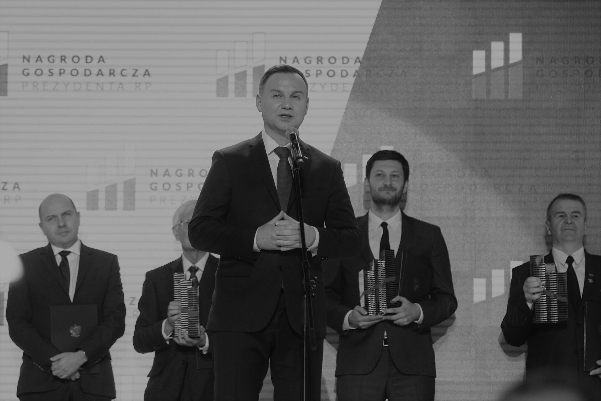
- Economic Award of the President of Poland at Kongres 590
- Development of a new application area – repair of broken metallic connections in thin-layered electronic circuits
December
- Announcement of plans for the transition to the main market of the WSE
- Conclusion of a subsidy contract for a laboratory printer prototype demonstration project under the Regional Operational Program for the Lower Silesian Voivodship 2014-2020
2018


April
Appointment to the Supervisory Board of Wiesław Rozłucki – former president and co-founder of the Warsaw Stock Exchange
May
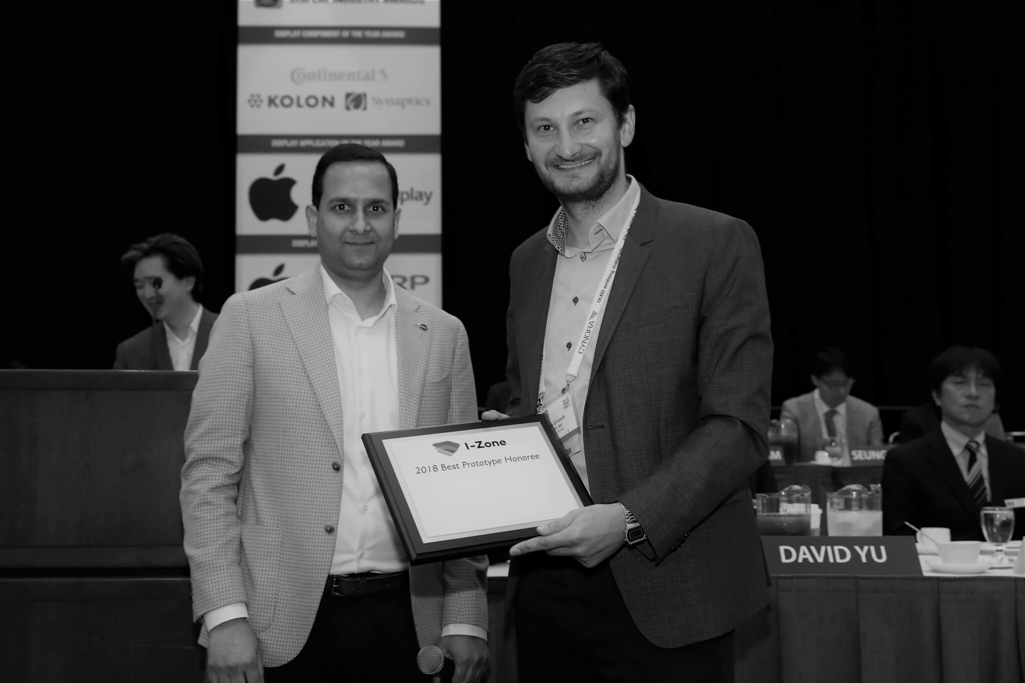
Award for one of the most promising technologies among the participants of I-Zone (innovation zone) being part of Display Week in Los Angeles
June
Establishment of an international Advisory Board – Harold Hughes became the first member
July
XTPL Advisory Board is joined by Amir Nayyerhabibi
September
- Private placement of 1 million Euro for the German fund – Acatis Investment
- Private placement of 1,05 million Euro for another German fund – Heidelberger Betailungsholding AG
November
Filip Granek wins EY Entrepreneur Of The Year Award!
December
XTPL opens the ranking of most eagerly investments in 2018
2019


February
- Establishing subsidiary XTPL Inc. in Silicon Valley, USA
- Debut of XTPL S.A. on the main market of WSE
May
Hiroshi Menjo joins the Board of Directors of XTPL Inc.
July
Acquiring PLN 10 million as a result of the issue of series S shares
August
Decision on licensing XTPL technology on the display market for use in the open defect repair.
September
XTPL forecasts a significant increase in the patent cloud
november
- Signing an agreement starting the evaluation of XTPL technology by BOE – the world leader in the production of modern displays
- Memorandum of understanding with Korean HPK Inc. opens the way to start business negotiations
2020


january
Herbert Wirth appointed new member of the Supervisory Board of XTPL S.A.
february
XTPL signed Technology Evaluation Agreement (TEA) with Suzhou Cowin laser Technology Co Ltd based in China
march
XTPL carried out three sales transactions of nanoink based on silver nanoparticles
june
- XTPL was awarded “The Best Investor Relations Website” in the categories “small enterprises” in the contest Złota Strona Emitenta XIII organized by the Polish Association of Listed Companies (SEG).
- On 30 June 2020, the Supervisory Board of XTPL S.A. appointed Jacek Olszański to the company’s Management Board. Since October 2018, he has served as the company’s financial manager.
- Beata Turlejska, a Managing Partner in the Leonarto VC. Fund, was appointed as a new member of the Supervisory Board.
july
The company adopted a resolution on the allocation of 48,648 series A registered bonds convertible into the company’s series U shares at an issue price of PLN 74 per bond. Overall, the company’s proceeds from the issue of shares and bonds are PLN 12,849,952.
november
XTPL has signed its first commercial contract for the UPD technology demonstrator – XTPL Delta Printing System for precise printing of micro-features, including conductive structures with the University of Stuttgart, Institut für Großflächige Mikroelektronik “IGM”
december
XTPL signed a contract for a subsidy in the amount of €2.6 million from the Polish National Centre for Research and Development (Narodowe Centrum Badań i Rozwoju) for the project on development of innovative technology of precise deposition of conductive grids for next-generation OLED displays.
2021


march
XTPL has established cooperation with Bandi Consortia to support the commercialization of XTPL technology on the Korean market.
april
- XTPL signed a contract for a subsidy in the amount of PLN 7.7 million from the Polish National Centre for Research and Development (NCBiR) for the project on development of breakthrough printing technology of 3D micrometric conductive structures using an innovative printhead capable of printing on non-planar substrates and compatible ink for printed electronics applications.
- XTPL starts cooperation with Yi Xin Technology, who will distribute the Company’s technological solutions in China.
may
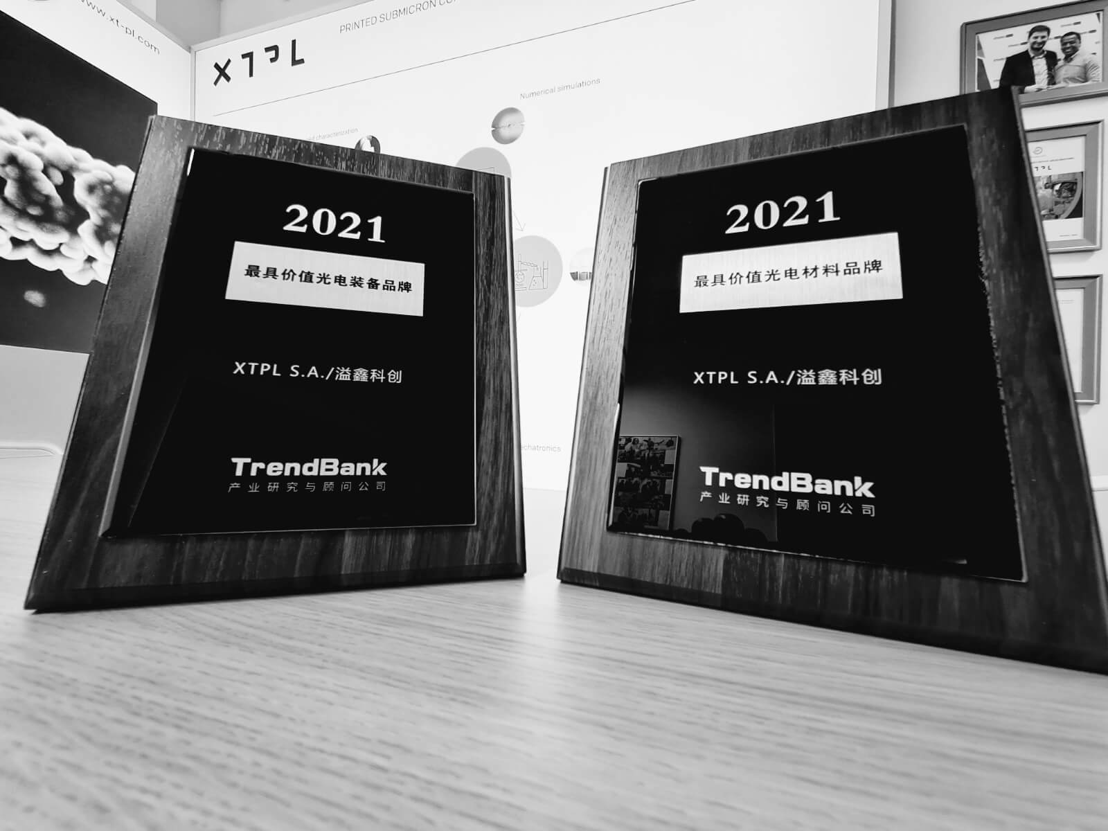
XTPL was awarded as “The most valuable optoelectronic equipment” and “The most valuable optoelectronic materials” during the Display & Touch Industry Conference 2021 (DTIC 2021)
July
- XTPL signed a sales agreement with the Karlsruhe Institute of Technology (KIT) in Germany for Delta Printing System.
- The Company started cooperation with Semitronics Sales Ltd, a highly-specialized distributor in Great Britain and Ireland region.
November
- XTPL S.A. signed an agreement with the Łukasiewicz Research Network – PORT Polish Center for Technology Development relates to the sale of Delta Printing System.
- The Company sold another Delta printer to the Bendable Electronics and Sensing Technologies (BEST) research group at the University of Glasgow
December
Scientists from the Italian University in Brescia acquire the Delta Printing System from XTPL S.A. for application in biosensors and bioelectronics for next-generation biomedicine
2022

january
- German merconics joins the group of distributors of XTPL solutions
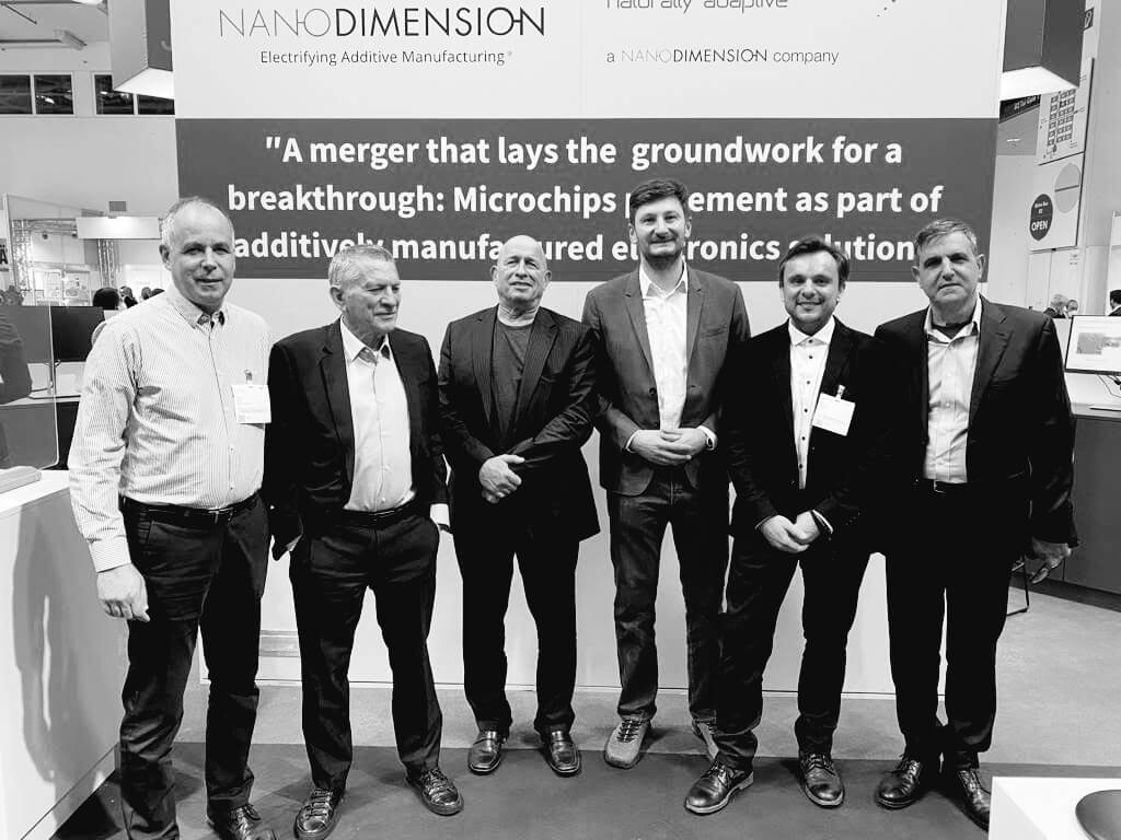
- XTPL and Nano Dimension announce collaboration to develop next-generation conductive nanoink
february
XTPL expanded its international distribution network by starting cooperation with Mumbai-based Vertex Global Solutions
march
- XTPL received a grant recommendation for the technological project “Building Active MicroLED displays By Additive Manufacturing”, for over EUR 4 million under Horizon Europe.
- XTPL started strategic cooperation with the Department of Information Engineering of the Italian University of Brescia (UniBS) in the field of new generation bioelectronics.
april
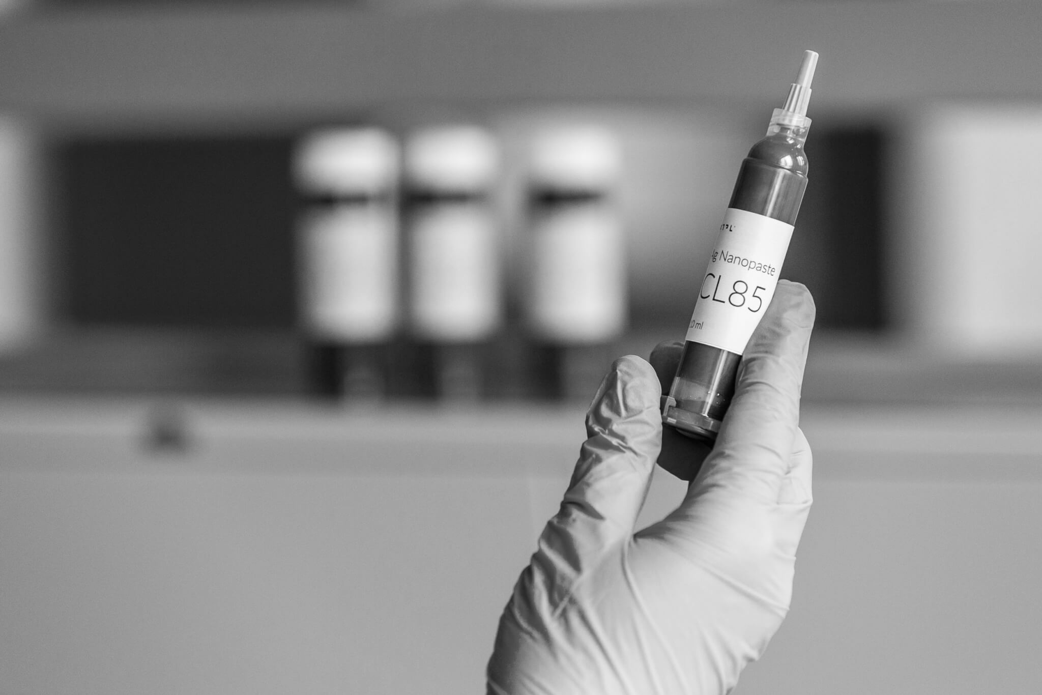
- XTPL signed an agreement with US-based nScrypt Inc. The agreement relates to the development and production by XTPL of Ag Nanopaste CL85 that will subsequently be added to nScrypt’s product offer.
- XTPL completed the first stage of the technological phase under
the agreement with Nano Dimension Ltd.