FAQ
We have answered some of the most frequently asked questions about our company and technology. Have a look and find out more.
What does the abbreviation “XTPL” mean?
The idea – that lies in the name of our company – describes also the origins of its existence. Extremely Thin Printed Lines – the effect of our first patented method that enabled ultra-precise printing of electrodes up to several hundred times thinner than a human hair. XTPL’s globally innovative technology was based on solving an interdisciplinary scientific and technological problem, covering challenges in fields such as solid state physics, inorganic chemistry, nanotechnology, material engineering, programming, machine learning algorithms, mechanics and electronics. At present the company expands its patent applications cloud and offers tailor made solutions for several industry sectors.
Why is XTPL solution a breakthrough?
Printing system designed by XTPL allows for ultra precise dispensing of a unique nanoink – specially composed in the laboratories of the company. The thickness and shape of individual structures created with this method, their length and distance between them depend on the specific application requirements. The main competitive advantage and breakthrough of the XTPL additive solution is unprecedented precision. Innovation developed by XTPL will contribute to the technological revolution that will enable the production of highly advanced devices using cheap and scalable methods of printing. Just as today we cheaply and quickly print newspapers and books, in the future we will print displays, solar cells, biosensors and other elements.
What is the difference between additive technology (XTPL) and subtractive technology?
Subtractive manufacturing is a process by which designed objects, patterns or structures are obtained by successively cutting material away from a solid block of material. This method – although allowing for high control and precision – is material- and time-consuming. It is also not as versatile as the change of design requires complex adaptations. It was though commonly used method as for some components there was not additive process available that could provide the desired results. Additive manufacturing is any process by which objects, patterns or structures are constructed by successively depositing (adding) material until it becomes a predesigned shape. Modern additive printing has always been very useful for rapid prototyping but it is starting to make strong impact on the manufacturing as well. XTPL provides disruptive manufacturable technology for adding conductive & nonconductive submicron structures for various applications with unparalleled precision, one that cannot be replicated by any other printing method in the world. Juts to give an example – microdots currently obtained on the market usually have about 50 um, the minimum is 20 um – while XTPL currently achieves dots with diameter of 1 um, and plans to go even below this limit. XTPL technology works on most substrates, even ones that are flexible and not flat. Additive process here allows then for ultimate simplicity & versatility. XTPL solution responds to market need of progressing miniaturization and provides highest performance, one that can be fabricated by inexpensive & scalable methods.

What are the key applications for XTPL technology?
What is unique in XTPL technology is the possibility of its application in many branches of industry. Our goal is to revolutionize in the first place the broad sector of PRINTED ELECTRONICS. Strong development of this market is due to the growing number of new applications of printed, flexible and organic electronics in various fields. XTPL technology will be used in many existing areas of printed electronics industry or – thanks to unprecedented precision of our solution – XTPL will enable the implementation of new ones. The technological revolution for this sector is based on enabling the production of complex and complicated devices with cheap and scalable methods. Just as today we cheaply and quickly print newspapers and books, in the future we will print displays, solar cells, biosensors and other elements.
Size of the market: 2017 – USD 29.3 Billion; 2027 – USD 73.4 Billion; CAGR 9.3% (forecast)
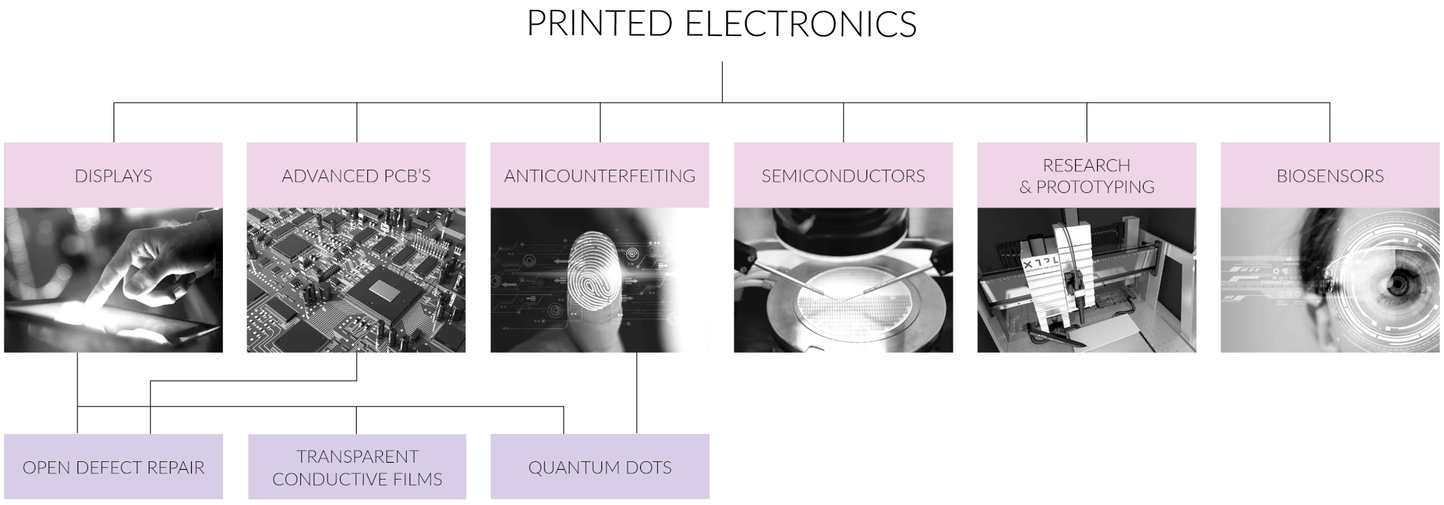
Below few examples showing applications in several areas of this market, worth billions of dollars each:
OPEN DEFECTS REPAIR
XTPL provides disruptive manufacturable technology for adding conductive nanostructures for various open defects repair applications with unparalleled precision. Our solution allows to repair interrupted conductive lines already in production stage using fast, simple & versatile method, leading to an overall lower production cost for the customers. XTPL provides the best competitive advantages from all current methods in the world and this factor is one of the reasons why here the Company expects its first industrial implementation.
TRANSPARENT CONDUCTIVE FILMS
The operation of displays, solar cells, touchscreens or smartphones include, among others, application of transparent conductive films (TCFs) with the highest possible neutrality to light (absorbed or emitted by the device) and, at the same time, with the highest conductance parameters. Currently, indium-tin oxide (ITO) TCFs are predominantly used. Due the limitations of ITO, technology companies around the world are looking for a next-generation TCF technology that could replace ITO. XTPL has developed such a technology providing: full transparency, excellent conductance parameters, low production costs due to the use of commonly available materials (i.e. silver) that can provide the sought-after technological independence from indium, flexibility of the conductive films, which will enable electronics manufacturers to develop and provide new generation of revolutionary solutions to customers.
SEMICONDUCTORS
XTPL solution meets the need of equipment manufactures in semiconductor sector for replacing photolithography with a simpler & cheaper method, yet one that allows for highest precision. Photolithography is highly complex, very expensive and not versatile technique, it requires both: an extremely clean substrate surface and ideal temperature conditions that are void of all contaminants, liquids & environmental hazards and is used only for flat surfaces in order to produce effective patterns. XTPL’s solution covers all those disadvantages providing sought after alternative in this sector.
What are the competitive advantages of XTPL technology in selected application fields?
PRINTED ELECTRONICS
- unprecedented precision of our solution
- enabling the production of complex and advanced devices with cheap and scalable methods
OPEN DEFECTS REPAIR
- repairing broken conductive lines already in production stage
- fast, simple & versatile method, leading to an overall lower production cost for the customers
- ultraprecise additive technology – saving material & time
- reduced width of the printed conductive lines and distances between them
- no toxic substances
TRANSPARENT CONDUCTIVE FILMS
- full transparency
- excellent conductance parameters
- low production costs due to the use of commonly available materials (i.e. silver) that can provide the sought-after technological independence from indium
- flexibility of the conductive films, which will enable electronics manufacturers to develop and provide new generation of revolutionary solutions to customers
SEMICONDUCTORS
- alternative to photolithography – simpler & cheaper method
- unparalleled precision
- technology providing ultimate simplicity, versatility & speed
- universality of patterns with no mask required
On what markets does XTPL operate?
The main directions of business development for XTPL are currently the USA and China. From the perspective of the technology XTPL develops, these are the most absorptive markets. We also see great potential in Singapore, Korea, Taiwan, Japan, South Korea, Germany, France, England, Switzerland, Italy, Finland, Israel, Austria and the Netherlands. We offer globally innovative solution and we have an interdisciplinary team of professionals effectively working in their careers on international markets. Our goal is to revolutionize at first sectors such as: printed electronics, flexible electronics, displays, smart glass, biosensors & anti-counterfeiting solutions. We see also vast potential in wearables, smart packaging, automotive as well as in solar cells.
What materials can you print with XTPL method?
XTPL method allows to print a large variety of available materials: conductive inks, nanoparticle based suspensions, semiconductor based suspensions, insulating inks, resists, solvent based inks and biological materials. In order to achieve outstanding results XTPL creates own conductive nanoink formulas based mostly on metallic nanoparticles (Ag, Au and Cu) and semiconductors (TiO2).
On what substrate can you print? Can you print on a flexible substrate?
We print on any type of substrate, conductive or non-conductive, e.g. glass, flexible foil (e.g. Kapton, PET, PEN, PDMS) or silicon wafers. In contrast to ink-jet, the substrate does not have to be flat, we can print on rough surfaces as well as on 2D and 2.5D surfaces.

SEM image of printed conductive silver line on 2.5D substrate
What patterns can be achieved by XTPL method?
XTPL developed innovative printing-head and dedicated nanoinks allowing for ultraprecise dispensing and obtaining designed microstructures for various applications. What makes the XTPL solution unique is ultimate simplicity, unparalleled precision, speed & versatility. The shape of individual structures created with this method, their width, length and distance between them depend on the specific application requirements. The feature size of printed structures is one of the key parameters in this revolutionary additive technology. The solution ensures micrometric scale of structures (1 – 100 um) required by many advanced industry sectors. XTPL disruptive technology works on most substrates, even ones that are flexible and not flat. The examples of possible patterns you can see the photos below:

SEM image of parallel lines printed with around 3 um width and 5 um distance between the lines

SEM image of the printed trail with 4 um width

SEM image of the segment of TCF printed on the glass using silver based nanoink designed & patented by XTPL. The width of the line: 6 um and interline distance: 500 um

SEM image of the pattern of XTPL logo composed from microdots dispensed on the glass. Dots currently obtained on the market usually have about 50 um, the minimum is 20 um – while XTPL currently achieves dots with diameter of 1 um, and plans to go even below this limit
Does XTPL printing process require multiple passes?
The printing process can be carried out in one or more passes of the printing head. Depending on the expected/desired result (e.g. height to width aspect ratio can be controlled by the number of passes). However, it is worth noticing that conductive traces can be obtained with a single pass of printing head.
Does XTPL printing process require sintering? How does XTPL perform sintering?
XTPL unique printing system allows to obtain very precise nonconductive & conductive structures. To obtain conductive structures XTPL uses special nanoinks synthesized in the company’s laboratories. The composition of XTPL’s nanoinks is each time precisely adjusted to specific requirements and its formulation is protected by an international patent application. In case of conductive structures – essential in applications such as TCFs for touch screens or repairing broken metallic paths in fine electronics circuits (open defects repair) – sintering is required. In this case XTPL uses nanoinks with metal nanoparticles (e.g. Ag, Au, Cu). Since our printing method is very versatile and allows for obtaining conductive structures on any kind of conductive or nonconductive substrate (even flexible or not flat one) the company uses different types of curing depending on a specific application. The process of sintering itself is crucial to meet conductivity requirements. The structures are heated in order to evaporate carrier solution and fuse individual particles together to form a continuous layer. Metal nanoparticles have melting points much lower than the corresponding bulk metal because of thermodynamic implications of the very large curvature of the particle surface. Traditional sintering, used extensively, relies on heat transfer mainly by convection and gives a high degree of control and predictability. However, many substrates such as coated papers and plastic films have softening points below the required sintering temperatures. Convection heating may in those cases cause deformation of the substrate and therefore selective heating of conductive layers with minimal heat transfer to the substrate is here more effective option. In main application area for XTPL technology, which is printed electronics sector, the most recent method is electrical sintering. During this process electric current is run through the conductive structure in which the heat develops because of the resistive losses. Only very small voltage can be applied here not to damage individual structures and the whole advanced circuit. Amongst methods of sintering used for conductive structures we can also apply plasma & chemical sintering, laser sintering (very flexible & precise method of concentrating high power to a very small area, although quite complicated and expensive), photonic curing (process of exposing the metal layer to pulses of high power light) and lastly rather unusual method of microwave heating (an interesting alternative when the printed structures are thinner than the penetration depth of silver at the frequency of interest). XTPL printing system allows to print variety types of inks, suitable for all types of curing. Thanks to that we are able to respond fast and flexibly to the needs of our clients. When it comes to nonconductive structures the process of sintering is not needed.
What is the speed of XTPL printing?
Current printing speed of XTPL method rages from 1 mm/s up to 250 mm/s for suitable inks. Depending on the properties of the ink and surface energy of the substrate typical speeds vary. Printing parameters are in all cases tuned for a specific ink and surface. High roughness and inhomogeneity in substrate thickness could limit the maximum speed of printing. XTPL printing head has a sensor with feedback loop to control the distance between substrate and printing nozzle and thus making printing possible even on non-flat and rough substrate.
Can you use XTPL printing method to repair broken conductive paths (so-called Open Defects)?
Yes, XTPL has developed an innovative printing head with dedicated nanoinks that allow defects in conductive paths to be repaired at low cost, with precision and speed unparalleled to any other existing solution.
The weakness of modern electronics lies in the fact that fine conductive structures in micro and nano scale used in integrated circuits, LCD and OLED displays, solar cells, advanced PCBs, etc. are highly prone to damage. Defects occur already at the production stage – the most common ones are: conductive paths broken due to a local lack of conductive material (open defects) and the narrowing of conductive paths (near open defects), which occurs when the width or height of the conductive path is less than required. This narrowing can degrade to complete breaking of path due to further production processes or exploitation. Removal of such defects is a multi-step and costly process, but in fact the repair is necessary in most cases as conductive electrodes are used in semi-finished products whose production price represents a significant proportion (even 50–70%) of the final product cost.
In addition, this problem is aggravated by the constant pursuit of miniaturization of electronic devices. This applies, for example, to integrated circuits – as they become smaller and smaller, it is increasingly complex to edit and repair metallic paths. Currently, the only developed method of editing structures with a width of less than 1 um is Focused Ion Beam (FIB). However, this method is not suitable for editing metallic paths with a length above 100 um, characterized by low electrical resistance. Moreover, it damages active electronic systems in integrated circuits (electrostatic discharge defects) and has other shortcomings which make it difficult or even impossible to repair integrated circuit.
In addition to FIB, other standard technologies for removing production defects include LVCD (Laser Chemical Vapour Dispensing) and DLD (Direct Laser Dispensing). All of these methods have their serious drawbacks: LVCD and FIB are extremely complex, LVCD and DLD provide only a limited possibility to obtain paths below 10 um while LCVD uses toxic and hazardous gases. Furthermore, all these three methods require a long repair time.
XTPL unique technology eliminates all disadvantages of the existing methods, and responds to the needs of the electronics industry in this regard as it allows broken conductive lines to be repaired already at the production stage, without complicated, slow and costly processes. Combined with optical detection systems already used in the market, our technology is a comprehensive solution to be implemented on production lines for e.g. solar cells, LCD and OLED displays, PCBs, MCM modules and integrated circuits.
XTPL solution takes into account all the requirements of the manufacturers: the greater overall length and smaller width of conductive lines with a simultaneous reduction of the distance between them, the need for reducing mechanical, thermal and electromagnetic stress in the production and repair processes, as well as increasing the cost-effectiveness. Our technology will ensure low-cost removal of production defects as well as high performance in industrial applications and no need for using toxic substances.
Does the company provide pre-sales support and samples made using XTPL technology?
Yes, the implementation of specifications and technological tests for potential clients are the key phases of most negotiations. In this way we confirm the unique capabilities of the XTPL technology for specific industries. Many industry sectors have already challenged us to address specific technological problems it is faced with. We take up those challenges, each time optimizing and calibrating our technology and its individual parameters to suit the particular sector. For the purpose of fulfilling of the specifications received, XTPL’s application laboratory conducts test and provides samples obtained with our unique technology. Having processed, measured and verified the properties of the samples, XTPL returns the output with a final report for the customer.
Is it possible to adapt and modify XTPL products to meet the specific customers’ needs?
Yes, the company aims to provide unique printing heads – each time designed & dedicated for specific application field – as well as compatible, precisely adjusted nanoinks. XTPL’s key objective is to develop & implement tailor made solutions in terms of nanoprinting and ultraprecise dispensing for several sectors such as: printed & flexible electronics, displays (open defect repair, transparent conductive films, quantum dots) semiconductors, advanced PCB’s, biosensors, smart glass & anticounterfeiting solutions.