Asian giant in negotiations with XTPL
XTPL, which specializes in nanoprinting of ultra-thin conductive lines, is on the verge of its first commercial contract abroad. One of the global leaders in the sale of machines for display production, valued at over USD 9 billion, has just started negotiations with the company. This is an effect of the previous work with the Chinese company on a proof-of-concept project. At present, XTPL is engaged in similar work for several dozens of other potential partners from around the world.
The contract to be negotiated by XTPL and the listed Chinese giant relates to the use of XTPL technology in the area of repairing broken metallic paths (“open-defect repair”) in thin-film electronic circuits. Chinese player, as one of the world’s leading suppliers of display production technology, aims to implement XTPL’s unique solutions in its technological lines.
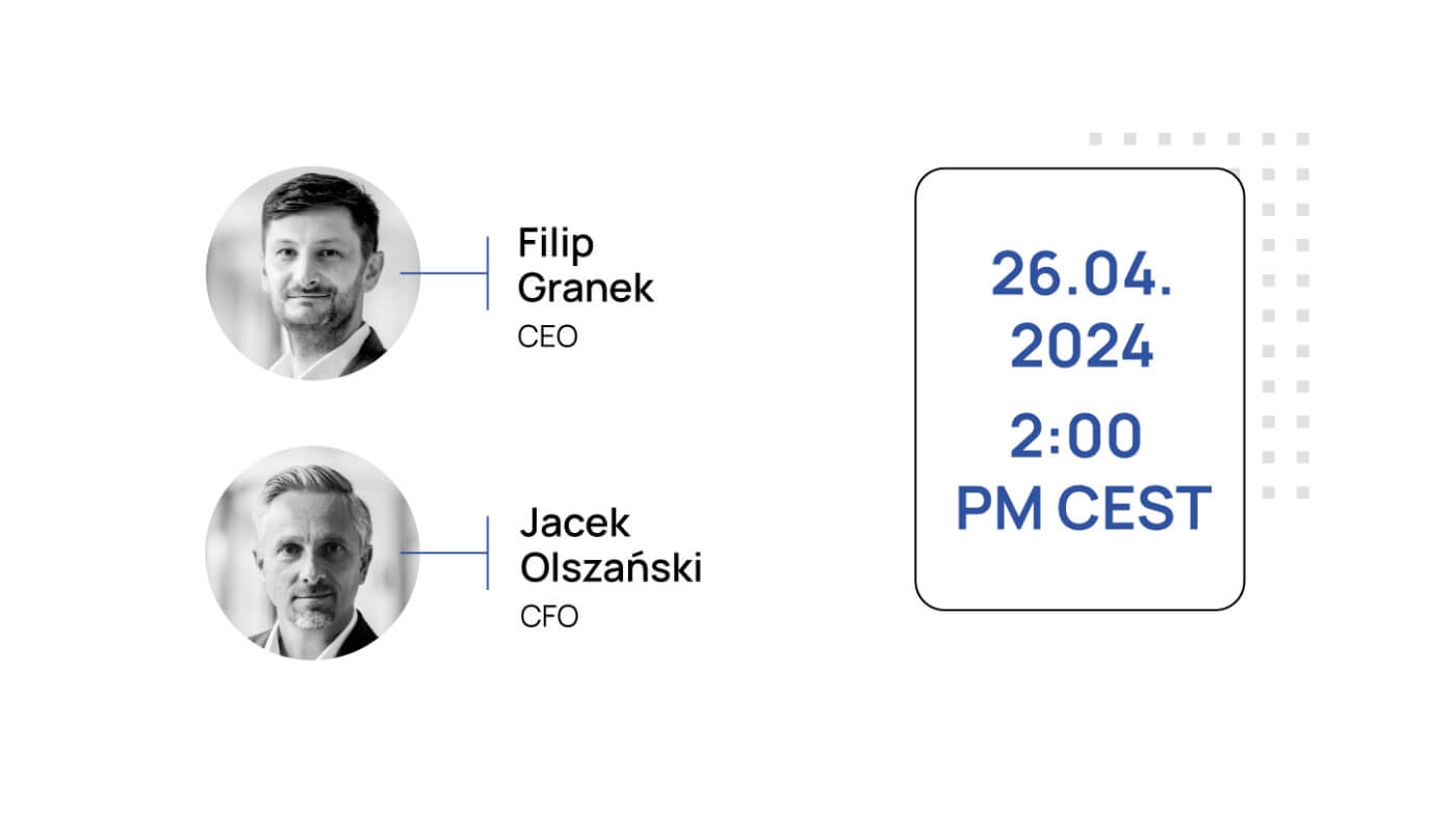
– For several quarters now we have been working hard to commercialize our nanoprinting technology. We know how to meet the challenges of our Chinese partner, who in March provided us with a technical specification, defining exact requirements for the technology he was looking for. A few weeks later XTPL application laboratory sent to China the work results which satisfied the manufacturer’s requirements. The samples were evaluated very highly, which resulted in an invitation to negotiate the terms of a commercial contract. In the recent weeks, several other large industrial players from around the globe have received samples from our laboratory. We are working on progressing to commercial contract negotiation phase with these firms as well – says Filip Granek, PhD, CEO of XTPL.
The size of the open-defect repair market is estimated at approximately USD 4.5 billion with approx. 7.5% CAGR. The end customers for this type of solutions primarily include manufacturers of TFT/LCD displays, silicon solar cells, integrated circuits and advanced PCBs. The technological solution developed by XTPL would be used for removing defects occurring already at the production stage and is expected to outperform the existing methods. Why? Due to its technical and operating parameters, namely: lower costs, lack of toxic chemicals and speed of application.
– This is just one of many fields of application for XTPL technology. Due to the platform character of XTPL solutions, we are verifying subsequent application segments in industries with a high-market potential. For example, we are focusing on: biosensors production, widely understood printed electronics, anti-counterfeiting solutions, smart packaging and semiconductors – Filip Granek notes.
After Harold Hughes, a long-standing CFO of Intel, had joined the Advisory Board of XTPL, the company has been even more active also in the Silicon Valley. This is where the company will be looking for its future commercial partners. In the United States, XTPL technology has already earned its reputation: at the recent Display Week show (with the main exhibitors being: Apple, Samsung, LG), the company was awarded in the category of the most promising technology.
Conductive lines printed using the XTPL method already now achieve parameters below 100 nm – this is an unparalleled precision which cannot be achieved by any other printing method in the world. Big industry needs our solutions, and negotiations with the Chinese partner is just the beginning
SAYS FILIP GRANEK